The bridge is four transistors. Something has to tell them when to turn on and off, several hundred thousand times a second, in the right order and with the right gaps. That is the driver, and without it the power section is a box of parts.
What it is and why
It finds the frequency. A Tesla coil's resonant frequency is not a number you can set once, because the arc changes it while it runs. So the driver measures the current in the tank, through a ring called a current transformer, and switches in step with what it finds. That loop, current in, gates out, current in again, is what keeps the bridge on the coil's frequency instead of on one you guessed.
It fires early. By the time the driver has decided and the signal has got to the gates, the current has moved on. So the driver deliberately switches before the moment it wants, by a lead it is given. Getting this wrong in the late direction destroys transistors.
It decides when to stop, and there are three separate reasons it might. The interrupter, or on a QCW the modulator, says when a bang begins and ends. The current going past a threshold ends it early, because nothing else in a doubly resonant coil limits that current. And the board watches its own supply rail: if that sags far enough the driver shuts itself down mid-bang, which is a failure that looks nothing like a supply problem from the outside.
It delivers the charge. A gate is a capacitor and a transition is a lump of charge moved into it and back out again, at the coil's frequency, for as long as the bang lasts. Making that fast enough is the fourth job, and it is the one that stops being a detail on a machine whose bangs are milliseconds rather than microseconds.
And what comes out is not a signal straight to the gates. It goes through a small transformer, because the top two transistors have their emitters sitting on the switching node, which is swinging by hundreds of volts. You cannot wire logic to a point that moves like that, so the signal is passed across magnetically. Three of the four jobs are settled on the board. This last one is settled past its edge, and only the part that holds a gate down when the drive is absent belongs to the driver itself.
What one actually looks like
A small board, a hand's width or so, well away from the power section and connected to it by a few wires. The signal runs across it in one direction:
feedback ring -> burden -> comparator -> logic -> output stage -> GDT -> gates
                               ^
protection ring -> burden -> OCD          interrupter -> enable
Somebody drew a board that way on purpose. Dawid Krajcarz publishes the driver from their own coil as drobotk/drsstc-driver, KiCad sources under an MIT licence, and the sheet is partitioned into labelled boxes that come out very close to the paragraphs above: Feedback, UVLO, Main logic, Interrupter, Output, Power. It is not a UD and it is not a clone of one. The credits name Ward, Finn Hammer, Slawinski, Anderson, Goodchild and Gao, and say the design it took most from is a project by Mike on the forum.
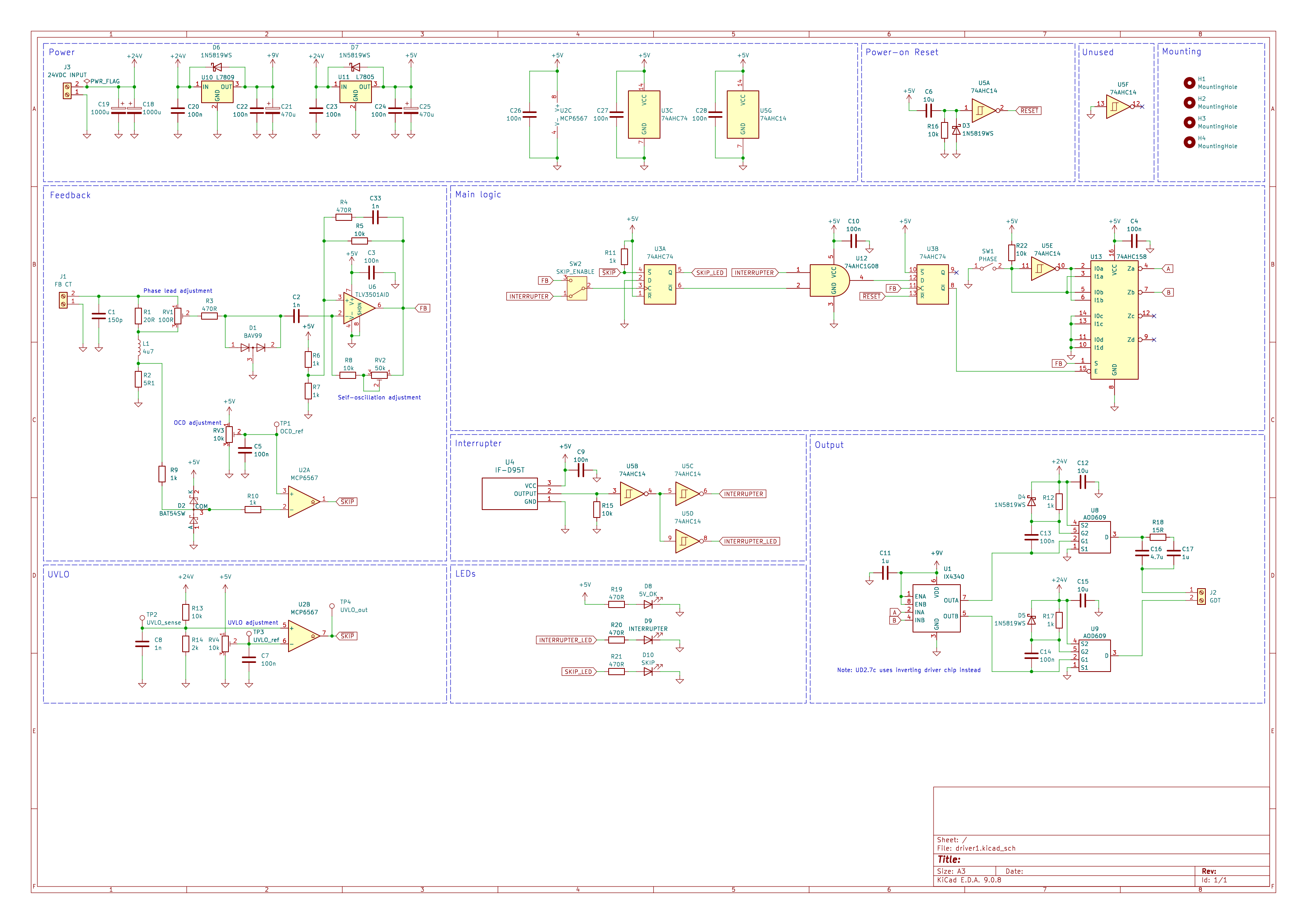
Three things on it are worth taking, and one of them argues with this site.
- The parts doing the deciding are comparators, which is the one decision this page says it is enough to make. A TLV3501 on the feedback, an MCP6567 on the overcurrent and another section of it on the undervoltage. The 74AHC14s are on the fibre receiver and in the logic, where a wandering threshold costs nothing.
- The lead is a knob rather than a part or a number.
R120R in series withRV1, a 100R potentiometer, and a fixed 4.7 µHL1, described in that board's own notes as "Phase lead adjustable with a potentiometer, no need for a tunable inductor". The UD line fixes the lead as an inductor you fit and the UD3 sets it as a time in nanoseconds; this is a third answer, and it is the cheapest of the three to change. The same list claims a reason for needing less of it, "74AHC high speed logic, less phase lead needed", which is the propagation delay of the chain showing up in the lead budget rather than in the parts list. - And it takes one ring, not two. The first line of the feature list is "Single CT input for both clock and overcurrent detection", and the sheet shows it:
J1markedFB CT, one 5R1 burden, and that same node running to both comparators. The paragraph below says two rings and means it. What the drawing adds is that the single input is a position somebody can hold deliberately in 2026, with the tradeoff in front of them and the UD3 making the same choice, rather than a corner cut by somebody who had not thought about it.
Two rings feed it, not one. The first says where the current is, for the frequency and the lead. The second says how big it is, for the protection. It is tempting to take both off the same ring and it is the wrong economy, for a reason worked on the ring's own page.
The interrupter comes in on fibre, or it should. A copper input is a wire from your low voltage logic into a machine that is radiating hard, and the fibre is there for isolation rather than for noise immunity alone. What it guarantees, and the rule that a broken link has to mean off rather than on, is the fibre and the fail-safe rule.
The frequency it is chasing is not one frequency. Coupled to a secondary the pair has two resonances rather than one, and which of them the driver lands on is a decision somebody makes rather than an accident; there is no secondary frequency is the whole of that. On a ramped machine it then moves while the bang runs, 390 kHz down to 330 on one published coil and 413 to 377 on another (the frequency slides down the ramp). Tens of kilohertz inside a single bang is why the first job cannot be done with a number you set in advance.
Steve Ward's open UD line is the reference every other driver gets described against, whether a builder runs one, a clone, or something of their own that is explained by how it differs. He published the design on his own site in 2008. The revision with a schematic, board files and a bill of materials published against it is UD2.7, on loneoceans. Daniel Marks rebuilt that revision through-hole as UD2.9, in the DRSSTC PCB Pack and under CC-BY-SA. Waska Labs carries the line on as UD29X, Phillip Slawinski's UD+ replaces the discrete logic with a CPLD, and Netzpfuscher's UD3 replaces it with a processor, which is the board this corpus keeps coming back to for what a shipped default costs you.
Which revision you are holding changes the part numbers but not the logic, and that matters the first time you follow somebody else's modification: the UD boards. It matters a second time when you take a board's shipped settings as a starting point, because those were typed against whatever coil the author had, and a programmable board will report back the number you set whether or not the hardware behind it took it.
The one decision this page is enough to make
Whether the parts doing the deciding are comparators.
A Schmitt trigger's thresholds wander with temperature and supply voltage. The driver needs a predictable threshold in two places, deciding when the current crossed zero and deciding when it is too high, so both want proper comparators. Using a 74HC14 is a design that can work rather than one that will.
Everything else, the lead network, the feedback strength, the protection behaviour, is a decision with a number attached and it is inside the driver.
What will get you
How to probe one of these boards anyway, and where a differential probe stops being optional, is with the scope.
What goes wrong
- The coil will not start, or runs at a frequency nobody asked for. Feedback. The current transformer's winding direction is the ten-second check.
- Transistors die at one tuning and survive at another. The lead, in the late direction.
- The protection never fires. It is a threshold, not a knob position, and it is not a setting.
- A board that worked stops the moment a probe touches it. See above.
- The bang starts correctly and dies partway in, at the same point every time. Not the protection and not the feedback: the driver's own supply rail sagging into its undervoltage lockout while the bang runs. The gate waveform captured at the start of a bang looks perfect, which is what makes this one read as a mystery. Put the scope on the rail rather than on the gate, for the whole length of a bang.
- It runs, but at a frequency that is not the one you tuned for. There are two to land on and the driver picked the other, which is not a fault but a choice somebody did not make.
- The gates look nothing like squares. That is the loop past the board's edge rather than the board: reading a gate waveform for what the shape is telling you, and the gate loop is an RLC for the resistor that sets it.
- The first cycles of every bang are wrong and the rest are right. Expected, and it has a name: the loop has nothing to follow until there is current in the tank, so every bang starts open loop.
- The driver dies when an arc hits something earthed. A different failure from all of the above and it does not start at the driver: what a ground strike does to a DRSSTC.
Where next
- Inside the driver, the same board with the numbers.
- What a phase lead actually buys, the lead the second job above is given.
- Switching at zero is the failure case, because the obvious target for that lead is the wrong one.
- Scoping a coil without killing it, for the warning above and the rest of what a ground clip does.
- Converting a DRSSTC driver, what has to change on one of these boards to run a ramp.
The driver is the box at the bottom of every department diagram, with the gate transformer above it and the current transformers feeding it from the right.