Steve Ward's Universal DRSSTC Driver is the board the rest of the field is described against, directly, through a clone, or through a rebuild that is explained by how it differs. Knowing which revision you are holding matters, because the logic travels between them and the part designators do not always travel with it.
What it is and why
One board doing the four driver jobs. It finds the coil's frequency, from a current transformer through a comparator. It advances the switching instant, with a phase lead made of a series L + R in place of a bare burden resistor. It decides when to stop, on the interrupter's enable or on current. And it delivers charge into the gates, through an output stage into a gate drive transformer.
On the UD2.x boards the first and third of those get a current transformer each, one ring for feedback and a separate one for protection, which is two rings, not one. The UD3 puts both jobs on a single input by design, and that page carries what the sharing costs. So the two rings are a property of the analogue boards, not of the line.
The reason the family is worth knowing as a line rather than as a product is that the comparator and flip-flop core did not change through 2.1, 2.5 and 2.7. Gao Guangyan's change list from UD2.0 to UD2.7A is regulators, layout, solder pads, board size and an under-voltage lockout, and he says the earlier work by others was small fixes, an extra fibre input and component placing (loneoceans). A modification published against one revision therefore transfers legitimately to another. Two members of the list are outside that: the UD+ replaces the discrete logic with a CPLD and the UD3 replaces it with a processor.
The revisions
- UD1.3b, Ward's own, published on his site in 2008 with schematic, board files and a parts list. Primary current feedback, a flip-flop, an optical interrupter input, overcurrent detection and a MOSFET-driven gate drive transformer output, and no phase lead.
- UD2, Ward again, adding adjustable lead compensation through a variable inductor. loneoceans credits the idea of adding lead to the feedback signal to Finn Hammer, who called it the Prediktor.
- UD2.1b, from Phillip Slawinski and Bart Anderson. Ward's own published design files stop at the UD2.1 revB schematic of March 2011, which is where the phase lead page takes his bill of materials from.
- UD2.5, from Eric Goodchild. It added the Industrial Fiber Optics receiver alongside the ST one, a test point for the overcurrent detector, and error fixes. Two independent pages name him: loneoceans in the history section above, and Daniel Marks in the DRSSTC PCB Pack README.
- UD2.7, Gao Guangyan's revision of Ward's UD2, published with Ward's permission and with all rights to the UD2 design left with Ward. Rev A and B are from September and October 2014, Rev C from January 2015. The switching 9 V regulator, the under-voltage lockout and the smaller board are his; so is the change of lead inductor family, from the Coilcraft Slot Ten parts in Ward's revB bill of materials to the Coilcraft Slot Seven 7M3 series. He gives the tested frequency range as 12 kHz to 1 MHz. He also publishes the schematic of every revision, A, B and C, alongside gerbers and a bill of materials, on his own page; go there rather than to any copy, because the terms he sets are download for personal hobby use and nothing broader.
- UD2.8A, Daniel Kramnik's revision of the UD2.7, in his own words a slight one: a jumper to pick between the two fibre inputs, SMA connectors instead of Molex, a barrel jack, surface-mount indicator LEDs and a relayout. The lead stays a tunable inductor, as on the board it revises.
- UD2.9, Daniel Marks' through-hole rebuild of the UD2.7C with a pulse skip jumper, in the DRSSTC PCB Pack, Kicad sources under CC-BY-SA. It keeps the 51 Ω feedback burden, the 5.1 Ω overcurrent burden, the Slot Seven 7M3 lead inductor and both fibre receivers. What it does not keep is the numbering, and that is the next section.
- UD29X, from WaskaLabs. Its README describes it as a standard surface-mount UD like the UD2.7C with differences: pulse skip inspired by Marks' UD2.9, the under-voltage lockout set by a fixed resistor instead of a trim pot, a single ST receiver instead of the ST and Industrial Fiber pair, 24 V DC input only, one gate drive channel, and breakout headers for extensions.
- UD+, Phillip Slawinski's. Freewheeling: over current it turns one half bridge off and lets the current circulate rather than cutting the bang. The deeper change is that the 74-series logic is replaced by one CPLD written in VHDL, with the sources published. Its lead inductor is not fixed by the line either: the board takes Slot Ten or Slot Seven parts, and the working combinations Slawinski lists for CM600 and CM300 modules are Slot Ten.
- UD3, Jens Kerrinnes' programmable driver, built on Ward's work and published as Netzpfuscher/UD3. Interrupter on board, a command line, USB-MIDI, autotuning, telemetry, master and slave. This is where the line gives up the inductor and sets the lead as a time instead of an angle, in nanoseconds. It is a different kind of board from the ten above it, and what it ships set to is read out of its own source rather than documented here.
- Eastern Voltage Research's Universal DRSSTC Controller is not a revision in this line at all. It is a product sold alongside it, in a shielded enclosure, with two current sense inputs for 1000:1 transformers, coarse and fine overcurrent knobs, and it supplies the lead as socketed plug-in inductor modules, IND-1 to IND-8, chosen by the size of the switch (datasheet, March 2014 Rev 1). Note what the modules are not. Each is a range, IND-1 at 9 to 15 µH up to IND-8 at 60 to 100 µH, so the part is still tuned after it is plugged in; and IND-1's 9 to 15 µH is the same span loneoceans gives for the Coilcraft 7M3-123. What changes is that the inductor is socketed instead of soldered.
One of the eleven, with its silkscreen readable
One revision in that list comes with board artwork published under a licence that permits reuse, and it is the one the rest of this page is written against.
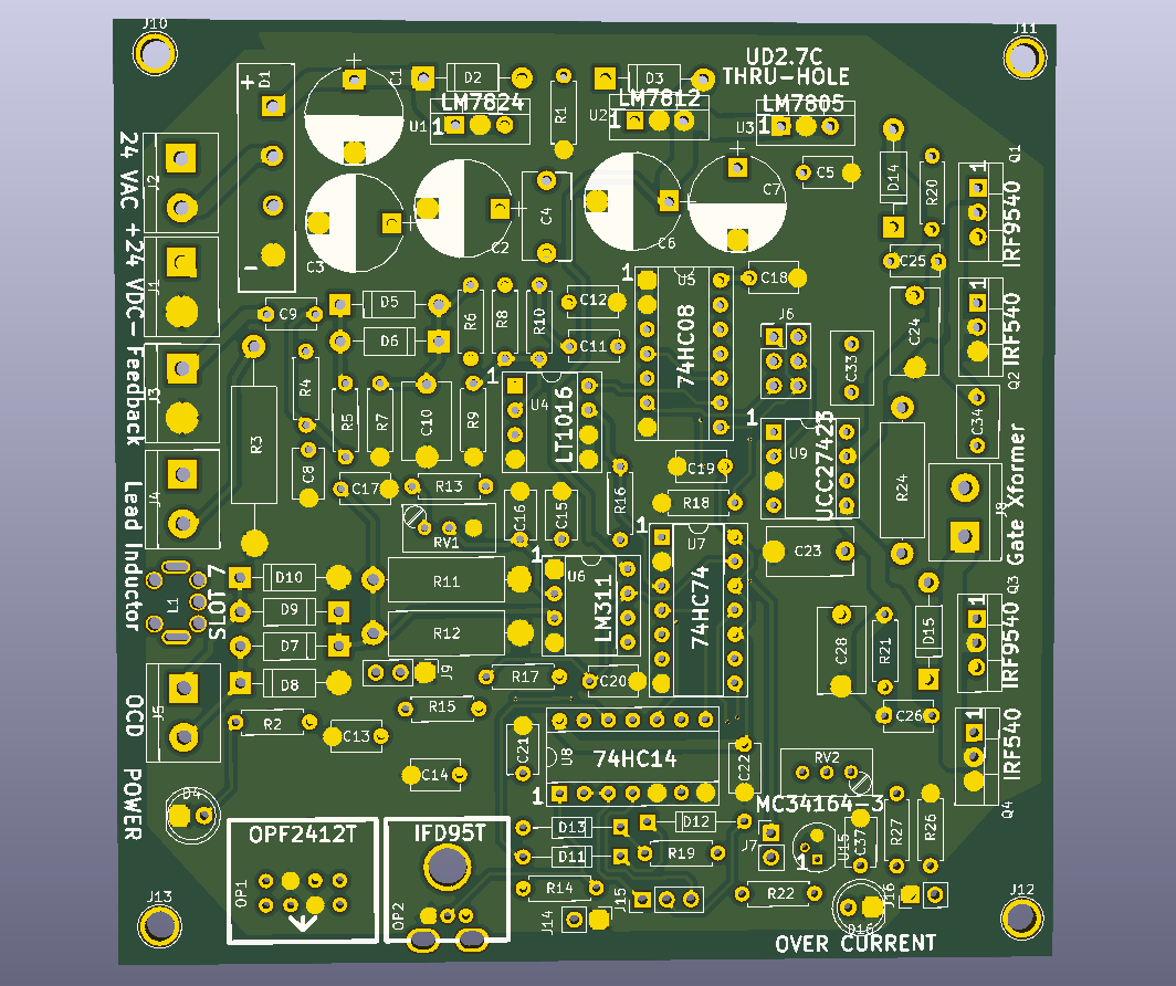
What the render shows that the list cannot. The left edge is the argument of two other pages, printed onto the board: Feedback and OCD are separate connectors, because they are separate transformers, which is two rings, not one. Lead Inductor and SLOT 7 are silkscreened on, which is what it means for a revision to fix the lead as a part rather than as a number, and what the UD3 gave up.
The UD2.9 board is this one with a group of parts added in the lower right corner and a thermal disable header beside them, which is why its render is not printed here as well: at this size the two are the same picture. The difference is legible on the schematics below, where it has net names on it.
The schematics themselves
The same pack publishes the circuit, not only the board, and under the same licence. These are the drawings the section below is read from.
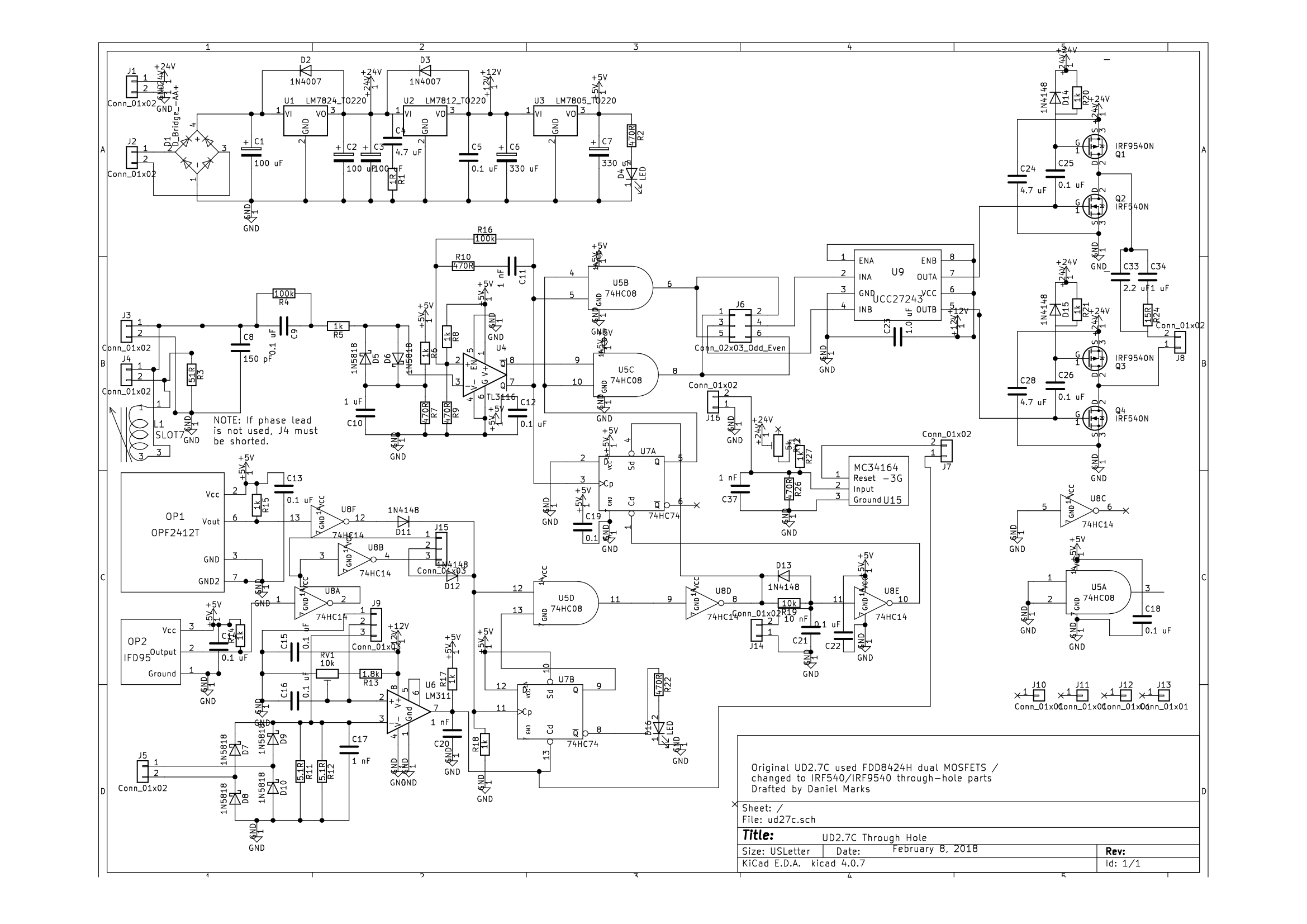
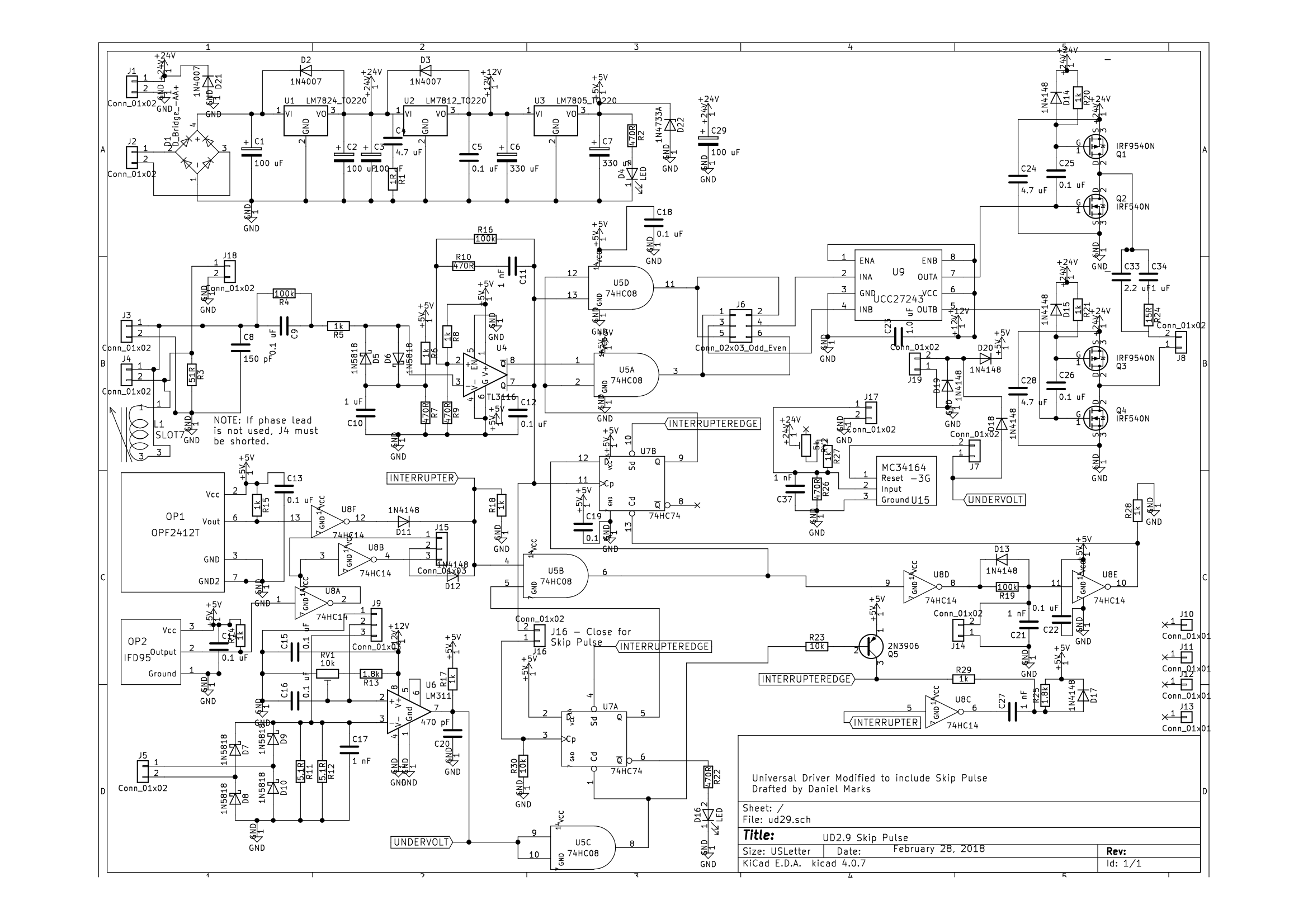
Set the two title blocks beside each other and you get the size of a revision in this line. 8 February 2018 and 28 February 2018, the same hand, twenty days apart. Everything up to the gate output is the same drawing. What is new is a handful of parts around a transistor and a header marked close for skip pulse, and on the board it is the group sitting in the lower right corner. What the added circuit is for, and why a QCW wants the other setting, is with the driver conversion.
The same pack has a third drawing, and it is what this line looks like once it leaves the analogue core. Marks also published a through-hole board for the UD3 idea, its title block reading Universal DRSSTC Driver ver 3 for CY8CKIT-059 and dated 1 April 2018, credited in the pack's own notes to Steve Ward and Jens Kerrinnes. It is not Kerrinnes' board, which is Altium sources carrying no licence. It is a third party's build of the same idea, drawn by the same hand that drew the two above, which is exactly what makes it readable beside them.
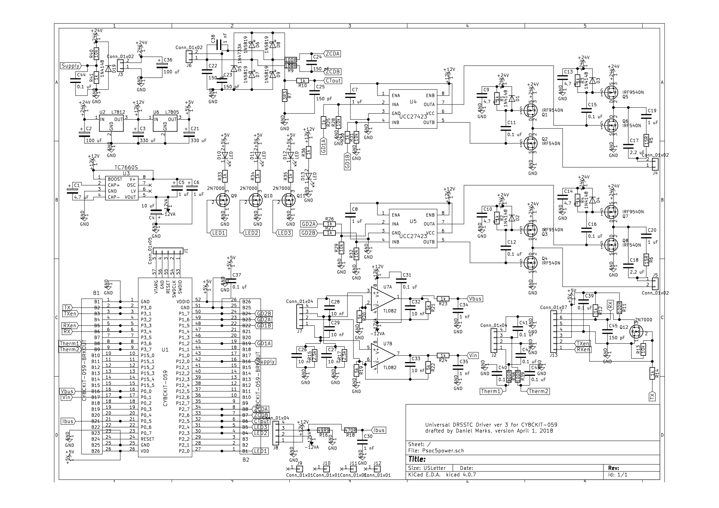
Three things are gone and three are new, and both lists are short enough to hold in your head.
Gone: the comparator, the flip-flop and the lead inductor. No TL3116, no 74HC74, no Slot Seven position on the board. A dev board sits in the middle of the sheet and every decision the two drawings above make in hardware has moved inside it.
New, and this is the one to carry: one ring input, three signals off it. J6 is the only current transformer connector on the board. Its burden is R7, 3R3, clamped by a 1N4733A and four 1N5819s. From that single node the sheet takes ZCDA and ZCDB through 100R and 150 pF, and CTout through 1k and 150 pF, and lands them on three separate pins of the dev board, B8, B7 and B6. So the thing this site keeps arguing with is not an economy somebody made at the bench. It is one connector, one burden and a fan-out, drawn that way on purpose, and what the sharing costs is two rings, not one.
New: it measures three things no UD2 measures. Therm1 and Therm2 arrive at J2 through 100R and 0.1 µF. A pair of TL082s at U7 turn J7 into Vbus and VIn. An Ibus chain runs from J8 through 49R9 and 470R into a 1 nF. The analogue boards know the primary current and nothing else about the machine. This one knows its own temperature, its bus voltage and its bus current, which is what autotuning and telemetry are made of and also why its settings live somewhere the silkscreen cannot tell you about.
New: the gate output is doubled. The UD2.7C drives one header. This board has the same output topology, four MOSFETs into a gate transformer through a series capacitor and resistor, built twice, at J4 and at J5.
And what goes to each of those terminals
The silkscreen names the connector and not what belongs on the end of it. Read the render at the top of this section against the schematic under it, and the whole board comes to nine terminals and two of them are only indicators.
Three of those are the ones the rest of this site spends pages on:
FeedbackandOCDare different holes. Two rings, two burdens, two jobs, and the reason is two rings, not one. A board that gave you one hole would be making the decision for you.Lead Inductoris a hole at all, which is the whole of what this line did until the UD3 stopped doing it. The schematic carries the instruction the silkscreen cannot: "If phase lead is not used, J4 must be shorted." Leave it open and nothing works, and nothing tells you why.Gate Xformeris the only thing the board drives. Everything else on the edge is an input or a lamp. What the driver actually decides is worked inside the driver.
What will get you
Removing the L+R section is not a simplification, and the board can show you so. The UD2.7 has a three pin header beside the inductor that selects R alone or R and L together. loneoceans scoped both on his own DRSSTC at about 380 kHz with the bridge at about 170 V of bus: with the lead jumpered out the collector to emitter transitions carry spikes he measures as "greater than 100V", and he says these can kill IGBTs because they are extremely sensitive to over-voltage. With a suitable inductor fitted and tuned, the spikes fall away.
The numbers
- Feedback burden: 51 Ω, 2 W. It is
R1on Ward's UD2.1 revB and on the UD2.7C bill of materials, andR3on Marks' UD2.9.C32is a 150 pF across it on the UD2.7C, andR2, the resistor that carries the signal on into the diode clamp before the comparator, is 1 k. - Overcurrent burden: 5.1 Ω on the same boards, with a second parallel pad provided for large machines.
R17andR28on the UD2.7C,R11andR12on the UD2.9. - Volts across that 51 Ω: loneoceans states the phase lead circuit runs a deliberately high voltage across the network, "~50+V across the 51R at 1A", and gives the reason: the comparator's delay from zero crossing to output is smallest when the signal arriving is large, which matters most in the first cycles of a bang. See the note below, because a live page reasons the other way from the same pair of figures.
- Lead inductor family: Coilcraft Slot Ten in Ward's UD2.1 revB bill of materials; Coilcraft Slot Seven 7M3 on the UD2.7 and on Marks' UD2.9; and either family on the UD+.
- The ceiling on an
L+Rlead: a quarter of a period, becausearctancannot exceed a right angle. Across the UD2.7's own tested band that is 20.8 µs at 12 kHz and 250 ns at 1 MHz [derived, the quarter period at the two ends of loneoceans' tested 12 kHz to 1 MHz]. That ceiling is what the line eventually runs into, and it is the numeric reason the last board in the line sets a time rather than an angle: above those frequencies no inductor buys the lead the wiki asks for, whatever it costs.
What is not established
- Whether any clone substitutes ordinary signal diodes for the Schottky pair that squares the feedback. Both open boards fit Schottky there: MBR0530 at
D1andD2on the UD2.7C bill of materials, 1N5818 or 1N5819 on Marks' UD2.9, with 1N4148 parts used elsewhere on both boards. Every bang starts open loop points at this page for the claim that a clone's changed feedback diodes are why it will not start on copied settings. This page cannot support it: no clone schematic has been read here, and the mechanism is not obvious either, since below a diode drop the clamp is not conducting and both boards behave alike. - Which board the Chinese clones actually derive from. Two open branches exist, Marks' pack and WaskaLabs' UD29X, and the UD2.7C is documented at length on loneoceans, which is where the UD29X README sends its own readers for the theory. Nothing read here settles which of the three any particular clone was traced from, and this page previously named the UD29X without a source.
What goes wrong
- A modification does not fit the board. The designators moved; the logic did not. Trace the function.
- Hard switching after a "cleanup" rebuild. The
L+Rsection was left out, or the header beside the inductor is selectingRalone. - The lead is right at one frequency and wrong at another. An
L+Rnetwork holds an angle, and the hardware needs a time. On a wide sweep that is the technique running out, not a component fault, and it is the reason the UD3 states the lead in nanoseconds. - A setting copied from another revision's thread does nothing you expected. Burden and inductor go together. Check which resistor the thread's board had before trusting its inductance.
Where next
- Inside the driver, what the board is doing and why.
- DRSSTC phase lead: what it is made of, which inductor to fit, and the inductor is the part these revisions keep changing.
Attribution: the revision history, the change lists and the UD2.7 figures are Gao Guangyan's, on loneoceans and in his bill of materials; the UD1.3b files are Steve Ward's; the UD2.9 board and its bill of materials are Daniel Marks', as are the UD2.7C through-hole rebuild and the CY8CKIT-059 board whose schematic is printed above; the UD29X is WaskaLabs'; the UD+ is Phillip Slawinski's; the UD3 firmware and wiki are Jens Kerrinnes', building on Ward. The quarter period ceiling and the four figures derived from it are ours, and are marked where they appear.